🚀 Future Explored: AI’s reimagined microchip
It could change the future of tech as we know it.
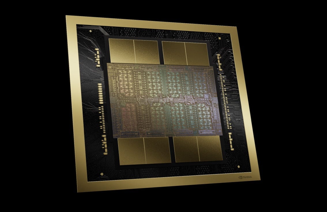
It’s 2028, and your tech startup has an idea that could revolutionize the industry — but you need a custom designed microchip to bring the product to market. Five years ago, designing that chip would’ve cost more than your whole company is worth, but your team is now able to do it at a fraction of price and in a fraction of the time — all thanks to AI, fittingly being run on chips like these.
Want to read this article on our website? Click here.
AI in chip design
By Kristin Houser
Microchips are the foundation of modern technology, and historically, the process of designing them has been left up to a few highly skilled engineers.
Today, powerful new AI systems are helping engineers with this process — and this collaborative approach could be the key to making sure we’re able to develop even more powerful AIs in the future.
Where we’ve been
Microchips are also called “integrated circuits” because that’s essentially what they are: electronic circuits integrated into a piece of semiconductive material, usually silicon (hence, “Silicon Valley”). Transistors and other tiny components control the flow of electrical signals along these circuits in ways that can process and store information.
While modern computers are incredibly flexible, not all chips are created equal and not all tasks work equally well with any chip. The design of a chip plays an absolutely crucial role in its performance and capabilities, and it’s up to chip designers to figure out which components should be included, in which places, so that the chip can do what it’s supposed to do as fast and as efficiently as possible.
These engineers also need to ensure the chip doesn’t cost more than it needs to, doesn’t use too much power, and can stand up to the environment it needs to work in — a chip in your car’s backup camera, for example, needs to be able to handle the sun beating down on it, as well as below-freezing temperatures.
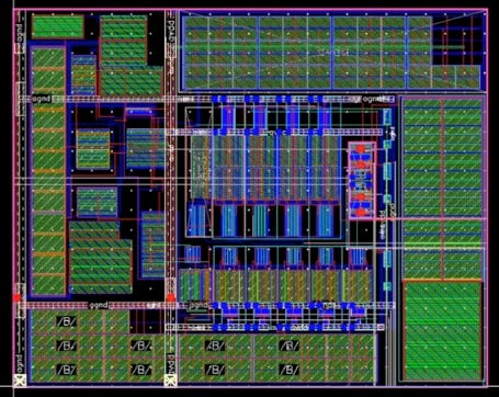
The very first microchips were designed literally by hand, but in the 1960s, engineers at computer companies started using software programs to design new chips.
Within a couple of decades, this approach — electronic design automation (EDA) — had become an entire industry of companies that develop software to not only design a chip, but also simulate its performance before actually having a prototype made, which is an expensive, time-consuming process.
“There are only a few manufacturing facilities in the entire world that make the vast majority of the integrated circuits we all use, and so the cost of actually making them is tremendous,” Rob Knoth, group director for strategy and new ventures at EDA company Cadence, told Freethink.
“In the semiconductor industry, we shoot for simulating 99% of the design in software,” he continued. “That way we know when we write that check for a billion dollars, the chip is going to come back six months later, and it’s going to work the first time.”
Even if a chip works the way it’s designed, though, that’s no guarantee that the chosen design is the best possible option for a specific application.
“When you go to lay out the chip, there are hundreds of parameters involved, and the number of permutations for moving blocks and creating a floorplan is an unfathomable number, probably close to the number of atoms in the universe,” Stelios Diamantidis, distinguished architect and executive director of the GenAI Center of Excellence at Synopsys, another EDA company, told Freethink.
Historically, an engineer could come up with maybe two or three options at a time to test, using their education and experience to guide them. They’d then (hopefully) arrive at a chip design that was good enough for an application in the amount of time they had to work on a project.
“There was no way of mathematically or otherwise proving that that was the best possible result,” said Diamantidis. “It was a good enough result.”
Where we are
Today, companies like Synopsys and Cadence are at the forefront of a new era in chip design, one where AI is helping engineers design integrated circuits at a scale that was previously impossible.
Many of the AI solutions the companies offer were created through “reinforcement learning,” which is when an AI model learns how to do something by repeatedly getting “rewarded” for producing better outputs, getting it closer to some goal.
This is the same technique that Google Deepmind used to create its game-playing AI, AlphaZero. In that example, they told the AI the basic rules of chess (what the board looks like, how each piece can move, etc.) and then let it play millions of games against itself. From the rewards or reinforcement it received when making advantageous moves, it evolved into a master of the game — in just nine hours.
“Essentially, we taught AI to play the game of chip design using Synopsys tools as its pieces on the chessboard,” said Diamantidis.
Just like AlphaZero, an AI trained to design chips can run through options far faster than an engineer can. As a result, engineers are now able to rapidly design chips that aren’t just “good enough,” but great.
“AI is already performing parts of the design process better than humans,” Bill Dally, chief scientist and senior VP of research at Nvidia, which uses products developed by both Synopsys and Cadence to design chips, told Communications of the ACM.
“Tools such as reinforcement learning find ways to design circuits that are quantitatively better than human designs,” he continued. “Sometimes, they come up with bizarre ideas that work because they operate completely outside the way humans think and go about designing chips.”
This ability to develop better chips, faster, couldn’t come at a better time.
Thanks to the recent AI boom, demand for new chips optimized to train and run AIs has skyrocketed — they’re also needed to guide autonomous cars, power humanoid robots, and more, and tech companies all need them before their competitors.
AI-based tools can not only design these chips faster, they can also optimize them for energy efficiency — AI itself is incredibly power hungry, and experts estimate that this is going to drive a 160% increase in energy consumption at data centers by 2030.
“The power consumption of data centers is directly dependent upon the power consumption of the integrated circuits that we’re making,” said Knoth. “It’s our job to make sure that we maximize the sustainability of AI … and AI itself can help us build better chips and build better data centers.”
Where we’re going (maybe)
While reinforcement learning has gotten us to this point, generative AI — models capable of generating brand-new content (text, images, music, videos, etc.) in response to user prompts — could take chip design to the next level.
The best known generative AI is undoubtedly OpenAI’s ChatGPT — a type called a “large language model” (LLM) — and it learned how to produce human-like text in response to prompts by training on essentially the entirety of the internet.
“When ChatGPT came about, it exposed everyone, including all our customers, to a new world of possibilities,” said Diamantidis. “We saw an opportunity to overlay generative AI on top of the reinforcement learning framework that we had built for optimization.”
“The first thing that was very clear that we could leverage was generative AI’s ability to understand and generate natural language,” he continued.
That led in November 2023 to the creation of Synopsis.ai Copilot, a version of Microsoft’s Copilot AI that is fine-tuned with documents about chip design. Synopsys has integrated the Copilot tool into its EDA products so that human engineers can now ask questions in natural language during the chip design process and receive easy-to-understand answers.
“Experience in chip design comes decades at a time, not one or two years at a time, so being able to onboard new talent and have them be more effective without constantly bringing in a more senior designer to guide them is hugely impactful, particularly in today’s talent shortage environment,” said Diamantidis.
Cadence is also exploring the potential of LLMs to aid with chip design. In September 2023, it unveiled a proof-of-concept system called ChipGPT that helps engineers review their initial code for a chip.
“Once the first draft … is created, engineers can use the LLM chatbot to interrogate the design, validate the design versus specification, explore and rectify issues, to prompt analysis tasks, and receive explanations in their natural language,” Steve Brown, director of strategic marketing at Cadence, wrote in a blog post.
Select Cadence partners, including Tokyo-based semiconductor manufacturer Renesa, are already implementing ChipGPT into their workflows. The company’s CTO, Shinichi Yoshioka, has said the AI was able to “significantly reduce the time from specification to final design.”
For more on this topic:
“We see large language models as an important piece of the puzzle that will shape the future for semiconductor design processes,” Yoshioka told Forbes
That future could include people who wouldn’t be able to design a chip today.
“I think we’re going to see a democratization process,” said Diamantidis. “The semiconductor industry has generally been associated with extremely detailed know-how and very high investments.”
“I think with AI, we’re going to be able to see innovators that may not be a large company,” he continued. “They may be five folks that got together with a great idea, they need a chip for it, and they will be able to design a chip.”
Google DeepMind is also driving to further democratize chip design.
In 2020, the AI research lab unveiled a reinforcement learning-based method for chip placement, the part of the design process focused on creating a floorplan for a chip. In 2021, DeepMind made the code open source, allowing anyone to access it for free, and in 2024, it gave the AI a name: AlphaChip.
AlphaChip has been used by researchers at NYU, Taiwanese semiconductor developer MediaTek, and Google itself, which used the AI in the development of CPUs for its data centers and three generations of its flagship AI chip, the tensor processing unit (TPU).
“AlphaChip outperformed the product of the human experts from the TPU physical design team, using the best available commercial tools, after they completed the lengthy traditional design optimization process,” Azalia Mirhoseini and Anna Goldie, senior staff research scientists at Google DeepMind and the lead authors on the AlphaChip paper, told Freethink.
Chip placement is just one part of the design process, but the researchers told Freethink that they are “excited about developing AI methods for other stages of chip design.” If they open source those methods, too, it could make designing a chip easier for everybody — not just those with the money to buy today’s EDA products.
“We would love to see a future where AI could help automate and optimize the entire chip design process for many kinds of chips,” said Mirhoseini and Goldie. “Imagine whenever someone wants to design a new chip, they could simply describe an application to a future version of AlphaChip, which then outputs a fully specified chip design that is ready for manufacturing.”
Kristin Houser is a staff writer at Freethink, where she covers science and tech.


